


Top China Manufacturer of Bi12GeO20 Substrate for Advanced Applications
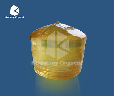
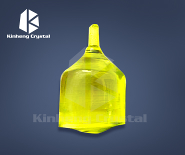
When I think about high-quality substrates for advanced applications, Bi12GeO20 substrate immediately comes to mind. Sourced directly from reliable manufacturers in China, this substrate is perfect for a range of uses including optoelectronics and semiconductor technology. With impressive thermal stability and excellent optical properties, Bi12GeO20 stands out in the market. I’ve seen firsthand how this substrate enhances performance in various devices, improving efficiency and reliability. As someone who values quality and dependability, I can confidently say that choosing Bi12GeO20 ensures you’re investing in a superior product. Whether you’re scaling up production or starting new projects, working with top-notch manufacturers in China means you’re getting the best in the business. Let’s elevate your applications with Bi12GeO20 substrate. You won’t be disappointed with the results!
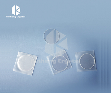
Bi12GeO20 Substrate Service Is The Best
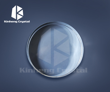
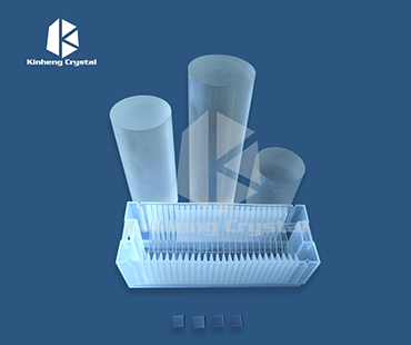
When it comes to advanced materials for electronic and photonic applications, the Bi12GeO20 substrate stands out for its exceptional properties. This unique substrate is known for its high optical quality, excellent electrical performance, and thermal stability, making it ideal for a variety of high-end applications, including laser devices and infrared optics. As global demand for sophisticated materials increases, sourcing the right substrate can significantly impact product performance and production efficiency. Our Bi12GeO20 substrate service offers customized solutions tailored to the specific needs of businesses around the world. We understand that each application has its unique set of requirements. With our advanced manufacturing processes and stringent quality control, we can produce substrates with precise dimensions and surface finishes that meet even the most demanding standards. Our commitment to innovation ensures that clients receive not only high-quality materials but also the latest advancements in substrate technology. Choosing the right supplier is crucial for your business's success. Our expertise in crystal materials and our dedication to customer satisfaction position us as a leading choice for global buyers. We are committed to providing timely delivery and competitive pricing, ensuring that you have the materials you need to stay ahead in this rapidly evolving market. Experience the difference with our Bi12GeO20 substrate service, designed to enhance your product performance and drive your business forward.
Bi12GeO20 Substrate Service Is The Best
| Parameter | Value |
|---|---|
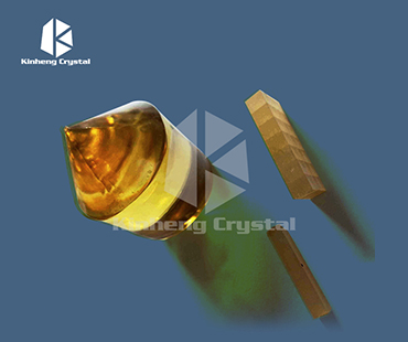
| Crystal Structure | Cubic |
| Lattice Constant | 1.204 nm |
| Thermal Conductivity | 0.9 W/(m·K) |
| Dielectric Constant | 30 |
| Band Gap | 2.1 eV |
| Main Application | Electro-optical devices |
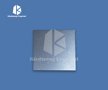
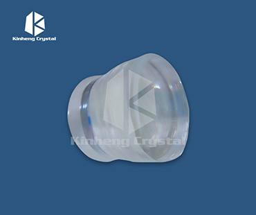
| Substrate Size Options | 2"x2", 3"x3", 4"x4" |
| Thickness Options | 0.5 mm, 1 mm, 2 mm |
| Surface Finish | Polished |
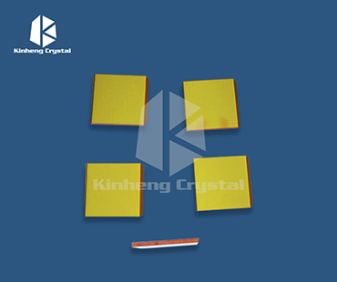
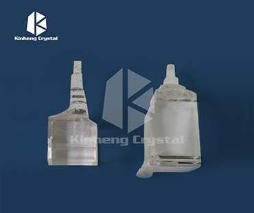
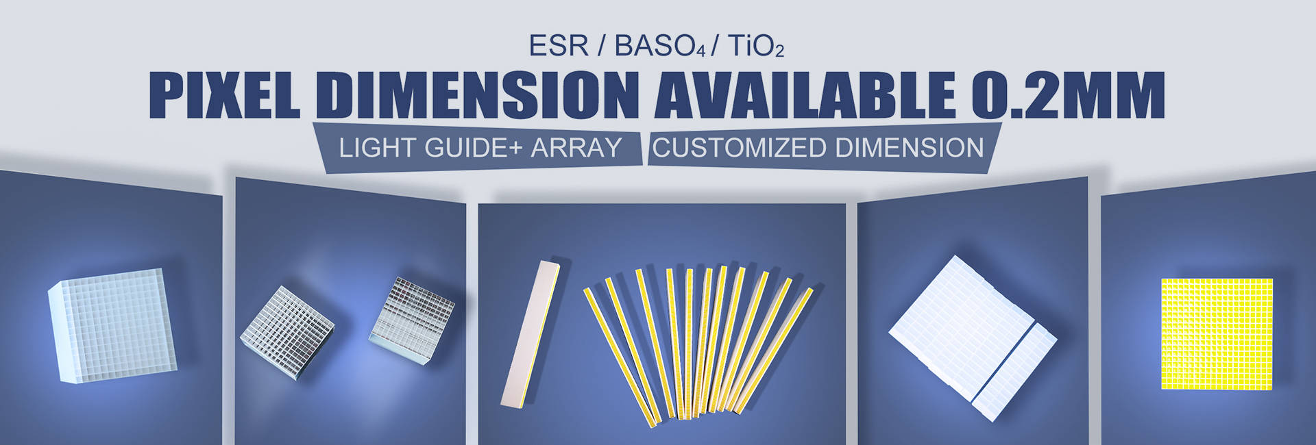
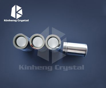
Related Products


Bi12GeO20 Substrate Market Leader Where Service Meets Innovation
Top Selling Products


- Related Blog
- Reviews
