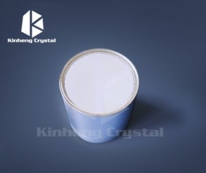
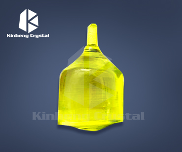
DyScO3 Substrate
Description
The single crystal of dysprosium scandium acid has a good matching lattice with the superconductor of Perovskite (structure) .
Properties
| Growth Method: | Czochralski |
| Crystal Structure: | Orthorombic, perovskite |
| Density (25°C): | 6.9 g/cm³ |
| Lattice Constant: | a = 0.544 nm; b = 0.571 nm ;c = 0.789 nm |
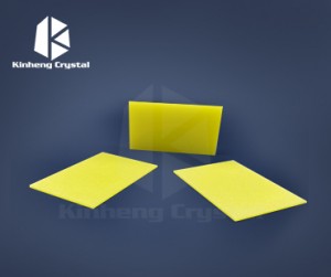
| Colour: | yellow |
| Melting Point: | 2107℃ |
| Thermal Expansion: | 8.4 x 10⁻⁶ K-1 |
| Dielectric Constant: | ~21 ( 1 MHz) |
| Band Gap: | 5.7 eV |
| Orientation: | <110> |
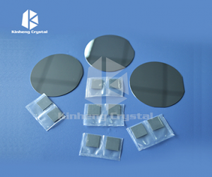
| Standard Size: | 10 x 10 mm² , 10 x 5 mm² |
| Standard Thickness: | 0.5 mm, 1 mm |
| Surface: | one- or both side epipolished |
DyScO3 Substrate Definition
DyScO3 (dysprosium scandate) substrate refers to a specific type of substrate material commonly used in the field of thin film growth and epitaxy. It is a single crystal substrate with a specific crystal structure composed of dysprosium, scandium and oxygen ions.
DyScO3 substrates have several desirable properties that make them suitable for a variety of applications. These include high melting points, good thermal stability, and lattice mismatch with many oxide materials, enabling the growth of high-quality epitaxial thin films.
These substrates are particularly suitable for growing complex oxide thin films with desired properties, such as ferroelectric, ferromagnetic or high-temperature superconducting materials. Lattice mismatch between substrate and film induces film strain, which controls and enhances certain properties.
DyScO3 substrates are commonly used in R&D laboratories and industrial environments to grow thin films by techniques such as pulsed laser deposition (PLD) or molecular beam epitaxy (MBE). The resulting films can be further processed and used in a range of applications, including electronics, energy harvesting, sensors and photonic devices.
In summary, the DyScO3 substrate is a single crystal substrate composed of dysprosium, scandium and oxygen ions. They are used to grow high-quality thin films with desirable properties and find applications in various fields such as electronics, energy and optics.