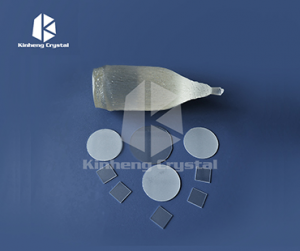
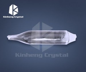
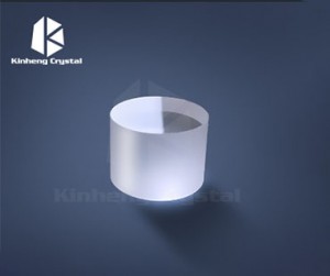
GaAs Substrate

Description
Gallium Arsenide (GaAs) is an important and mature group III-Ⅴ compound semiconductor, it's widely used in the field of optoelectronics and microelectronics. GaAs is mainly divided into two categories: semi-insulating GaAs and N-type GaAs. The semi-insulating GaAs is mainly used to make integrated circuits with MESFET, HEMT and HBT structures, which are used in radar, microwave and millimeter wave communications, ultra-high-speed computers and optical fiber communications. The N-type GaAs is mainly used in LD, LED, near infrared lasers, quantum well high-power lasers and high-efficiency solar cells.
Properties
|
Crystal |
Doped |
Conduction Type |
Concentration of Flows cm-3 |
Density cm-2 |
Growth Method |
|
GaAs |
None |
Si |
/ |
<5×10⁵ |
LEC |
|
Si |
N |
>5×10¹⁷ |
|||
|
Cr |
Si |
/ |
|||
|
Fe |
N |
~2×10¹⁸ |
|||
|
Zn |
P |
>5×10¹⁷ |
GaAs Substrate Definition
The GaAs substrate refers to a substrate made of gallium arsenide (GaAs) crystal material. GaAs is a compound semiconductor composed of gallium (Ga) and arsenic (As) elements.
GaAs substrates are often used in the fields of electronics and optoelectronics due to their excellent properties. Some key properties of GaAs substrates include:
1. High electron mobility: GaAs has higher electron mobility than other common semiconductor materials such as silicon (Si). This characteristic makes GaAs substrate suitable for high-frequency high-power electronic equipment.
2. Direct band gap: GaAs has a direct band gap, which means that efficient light emission can occur when electrons and holes recombine. This characteristic makes GaAs substrates ideal for optoelectronic applications such as light emitting diodes (LEDs) and lasers.
3. Wide Bandgap: GaAs has a wider bandgap than silicon, enabling it to operate at higher temperatures. This property allows GaAs-based devices to operate more efficiently in high-temperature environments.
4. Low noise: GaAs substrates exhibit low noise levels, making them suitable for low noise amplifiers and other sensitive electronic applications.
GaAs substrates are widely used in electronic and optoelectronic devices, including high-speed transistors, microwave integrated circuits (ICs), photovoltaic cells, photon detectors, and solar cells.
These substrates can be prepared using various techniques such as Metal Organic Chemical Vapor Deposition (MOCVD), Molecular Beam Epitaxy (MBE) or Liquid Phase Epitaxy (LPE). The specific growth method used depends on the desired application and the quality requirements of the GaAs substrate.