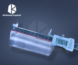
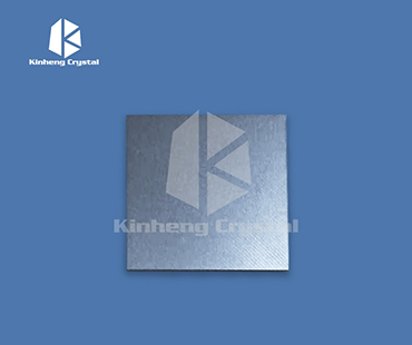
CZT Substrate
Description
CdZnTe CZT crystal is the best epitaxial substrate for HgCdTe (MCT) infrared detector because of its excellent crystal quality and surface precision.
Properties
| Crystal |
CZT (Cd0.96Zn0.04Te) |
| Type |
P |
| Orientation |
(211), (111) |
| Resistivity |
>106Ω.Cm |
| Infrared transmittance |
≥60%(1.5um-25um) |
| (DCRC FWHM) |
≤30 rad.s |
| EPD |
1x10⁵/cm2 <111>; 5x10⁴/cm2 <211> |
| Surface Roughness |
Ra≤5nm |
CZT Substrate Definition
CZT substrate, also known as cadmium zinc telluride substrate, is a semiconductor substrate made of a compound semiconductor material called cadmium zinc telluride (CdZnTe or CZT). CZT is a high atomic number direct bandgap material suitable for a variety of applications in the field of X-ray and gamma-ray detection.
CZT substrates have a wide bandgap and are known for their excellent energy resolution, high detection efficiency, and ability to operate at room temperature. These properties make CZT substrates ideal for manufacturing radiation detectors, especially for X-ray imaging, nuclear medicine, homeland security, and astrophysics applications.
In CZT substrates, the ratio of cadmium (Cd) to zinc (Zn) can be varied, enabling tunability of material properties. By tuning this ratio, the bandgap and composition of CZT can be tailored to specific device requirements. This compositional flexibility provides enhanced performance and versatility for radiation detection applications.
To fabricate CZT substrates, CZT materials are typically grown using various methods, including vertical Bridgman growth, moving heater method, high-pressure Bridgman growth, or vapor transport methods. Post-growth processes such as annealing and polishing are usually performed to improve the crystal quality and surface finish of the CZT substrate.
CZT substrates have been widely used in the development of radiation detectors, such as CZT-based sensors for X-ray and gamma-ray imaging systems, spectrometers for material analysis, and radiation detectors for security inspection purposes. Their high detection efficiency and energy resolution make them valuable tools for nondestructive testing, medical imaging, and spectroscopy applications.