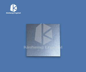
Ge substrate

Description
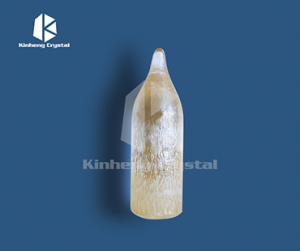
Ge single crystal is excellent semiconductor for Infrared and IC industry.
Properties
|
Growth Method |
Czochralski method |
||
|
Crystal Structure |
M3 |
||
|
Unit Cell Constant |
a=5.65754 Å |
||
|
Density(g/cm3) |
5.323 |
||
|
Melting Point(℃) |
937.4 |
||
|
Doped Material |
No doped |
Sb-doped |
In / Ga –doped |
|
Type |
/ |
N |
P |
|
Resistivity |
>35Ωcm |
0.05Ωcm |
0.05~0.1Ωcm |
|
EPD |
<4×10³∕cm2 |
<4×10³∕cm2 |
<4×10³∕cm2 |
|
Size |
10x3,10x5,10x10,15x15,,20x15,20x20, |
||
|
dia2” x 0.33mm dia2” x 0.43mm 15 x 15 mm |
|||
|
Thickness |
0.5mm,1.0mm |
||
|
Polishing |
Single or double |
||
|
Crystal Orientation |
<100>、<110>、<111>、±0.5º |
||
|
Ra |
≤5Å(5µm×5µm) |
||
The Ge Substrate Definition
The Ge substrate refers to a substrate made of element germanium (Ge). Germanium is a semiconductor material with unique electronic properties that make it suitable for a variety of electronic and optoelectronic applications.
Ge substrates are commonly used in the manufacture of electronic devices, especially in the field of semiconductor technology. They are used as base materials for depositing thin films and epitaxial layers of other semiconductors such as silicon (Si). Ge substrates can be used to grow heterostructures and compound semiconductor layers with specific properties for applications such as high-speed transistors, photodetectors, and solar cells.
Germanium is also used in photonics and optoelectronics, where it can be used as a substrate for growing infrared (IR) detectors and lenses. Ge substrates have properties required for infrared applications, such as a wide transmission range in the mid-infrared region and excellent mechanical properties at low temperatures.
Ge substrates have a closely matched lattice structure to silicon, making them compatible for integration with Si-based electronics. This compatibility allows the fabrication of hybrid structures and the development of advanced electronic and photonic devices.
In summary, a Ge substrate refers to a substrate made of germanium, a semiconductor material used in electronic and optoelectronic applications. It serves as a platform for the growth of other semiconductor materials, enabling the fabrication of various devices in the fields of electronics, optoelectronics and photonics.