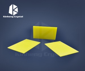
PMN-PT Substrate

Description
PMN-PT crystal is known for its extremely high electromechanical coupling coefficient, high piezoelectric coefficient, high strain and low dielectric loss.
Properties
| Chemical Composition |
( PbMg 0.33 Nb 0.67)1-x: (PbTiO3)x |
| Structure |
R3m, Rhombohedral |
| Lattice |
a0 ~ 4.024Å |
| Melting Point(℃) |
1280 |
| Density (g/cm3) |
8.1 |
| Piezoelectric Coefficient d33 |
>2000 pC/N |
| Dielectric Loss |
tand<0.9 |
| Composition |
near the morphotropic phase boundary |
PMN-PT Substrate Definition
PMN-PT substrate refers to a thin film or wafer made of piezoelectric material PMN-PT. It serves as a supporting base or foundation for various electronic or optoelectronic devices.
In the context of PMN-PT, a substrate is typically a flat rigid surface on which thin layers or structures can be grown or deposited. PMN-PT substrates are commonly used to fabricate devices such as piezoelectric sensors, actuators, transducers, and energy harvesters.
These substrates provide a stable platform for the growth or deposition of additional layers or structures, allowing the piezoelectric properties of PMN-PT to be integrated into devices. Thin-film or wafer form of PMN-PT substrates can create compact and efficient devices that benefit from the material's excellent piezoelectric properties.
Related Products
High lattice matching refers to the alignment or matching of lattice structures between two different materials. In the context of MCT (mercury cadmium telluride) semiconductors, high lattice matching is desirable because it allows the growth of high-quality, defect-free epitaxial layers.
MCT is a compound semiconductor material commonly used in infrared detectors and imaging devices. To maximize device performance, it is critical to grow MCT epitaxial layers that closely match the lattice structure of the underlying substrate material (typically CdZnTe or GaAs).
By achieving high lattice matching, the crystal alignment between layers is improved, and the defects and strain at the interface are reduced. This leads to better crystalline quality, improved electrical and optical properties, and enhanced device performance.
High lattice matching is important for applications such as infrared imaging and sensing, where even small defects or imperfections can degrade device performance, affecting factors such as sensitivity, spatial resolution, and signal-to-noise ratio.