


High-Quality Lithium Niobate Wafers from Trusted Supplier
As someone deeply invested in the semiconductor industry, I understand the critical role that high-quality materials like Lithium Niobate Wafers play in various applications. Our Lithium Niobate Wafers are crafted to meet the highest standards, ensuring exceptional performance in optical and electronic devices. When I say high-quality, I mean meticulously sourced raw materials and precision manufacturing processes that guarantee unmatched reliability and consistency. If you’re seeking a dependable supplier for Lithium Niobate Wafers, you’ve come to the right place. I take pride in providing superior products that can enhance your projects, whether in telecommunications, photonics, or other advanced technologies. By choosing our wafers, you’re not just getting a product; you’re investing in excellence and longevity for your applications. Let’s connect to discuss your specific needs and how we can support your success with our premium Lithium Niobate Wafers.


Lithium Niobate Wafers For the Current Year Trusted by Pros
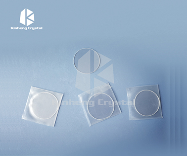
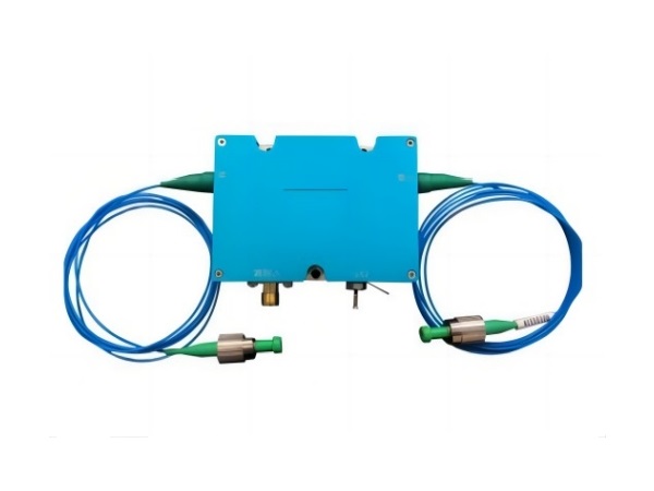
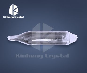
Lithium niobate wafers have become a focal point in various high-tech applications, ranging from telecommunication to advanced sensors. As industries worldwide continue to drive innovation, the demand for high-quality lithium niobate wafers is surging. Trusted by experts in the field, these wafers offer outstanding electro-optical properties, making them ideal for a wide range of applications, including optical modulators and waveguides. With their ability to operate over a broad spectrum and their superior piezoelectric properties, lithium niobate wafers are essential for companies aiming to stay ahead in the competitive technology market. For global purchasers, understanding the quality and specifications of lithium niobate wafers is crucial. High-quality wafers not only ensure the performance and longevity of devices but also enhance overall reliability. Companies looking to source these materials will benefit from working with trusted suppliers who prioritize stringent quality controls and advanced manufacturing techniques. By choosing reliable partners, businesses can secure materials that meet their precise requirements, thereby optimizing their production processes and driving innovation. As we move further into this year, the market for lithium niobate wafers continues to evolve. With advancements in material science and processing technologies, we are witnessing new opportunities for customization and improved performance. Buyers should remain vigilant, staying informed about the latest developments and fostering partnerships with manufacturers committed to excellence. The right choice of materials can pave the way for future successes in various technological endeavors, solidifying a company’s position in the global market.
Lithium Niobate Wafers For the Current Year Trusted by Pros
| Property | Specification | Applications | Notes |
|---|---|---|---|
| Thickness | 0.5 mm | Optical devices | Standard thickness |
| Diameter | 4 inches | Telecommunication | Common size |
| Crystal Orientation | Z-cut | Nonlinear optics | Preferred for Pockels effect |
| Flatness | < 0.5 μm | High precision optics | Critical for laser systems |
| Surface Quality | Grade 1 | Waveguides | Highest optical quality |
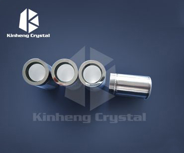
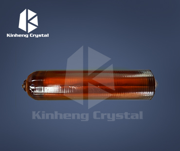
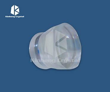
Related Products

Lithium Niobate Wafers Pioneers in the Field Now Trending
Top Selling Products

- Related Blog
- Reviews
